
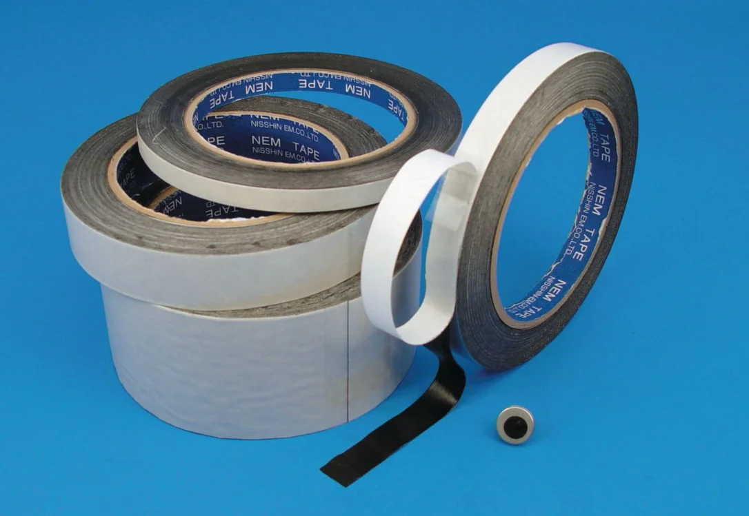
Description
This Copper/Nickel Tape from Electron Microscopy Sciences is designed for SEM applications, offering conductive properties essential for sample preparation. It features a 0.05 mm pad thickness, ensuring reliable conductivity for imaging. The tape is a crucial accessory for researchers in microscopy, providing a stable surface for mounting specimens.
- Copper/Nickel composition for effective conductivity.
- 0.05 mm pad thickness for optimal performance.
- Designed for Scanning Electron Microscopy (SEM) applications.
Enhance your microscopy workflow with this high-quality conductive tape.

Reviews
There are no reviews yet.